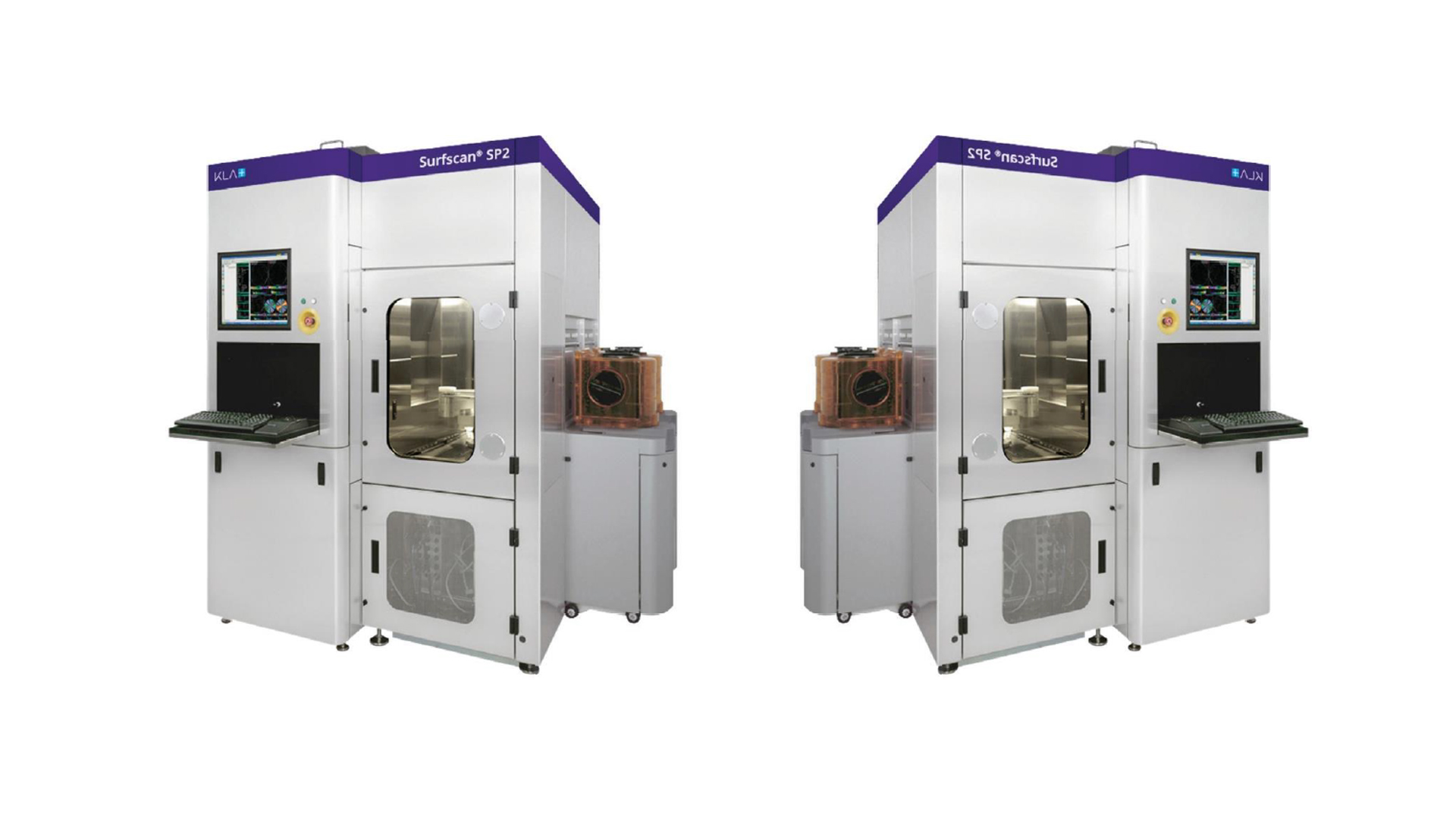
Surfscan® SP2 / SP2XP

Unpatterned Wafer Defect Inspection Systems
The Surfscan® SP2 and SP2XP systems are the 2nd generation of KLA’s revolutionary Surfscan SP1 platform for unpatterned wafer inspection.Incorporating revolutionary ultraviolet (UV) laser technology, new darkfield optics and advanced algorithms, the Surfscan SP2 finds defects as small as 37nm, and throughputs up to 2x faster than the prior-generation tool at the same sensitivity. Designed for emerging technologies such as RF, automotive, SiC, GaN, LED and mature process nodes to the ≥4xnm design rule, the SP2 facilitates the qualification and monitoring of processes and tools required by substrate, IC, equipment and materials manufacturers across the semiconductor ecosystem.
The Surfscan series unpatterned inspectors are designed to capture and classify critical defects in real-time on bare wafers, smooth & rough films and stacks, photoresists and litho stacks. By discovering and identifying critical defects and surface quality issues early on, the Surfscan tools enable faster identification of process and tool issues, driving faster ramp, higher yield and improved profitability. The SP2 Pro series tools satisfy R&D pathfinding applications and are equally suited to provide critical tool monitoring inspection points in a full manufacturing environment, all in a single tool.
1、Normal and Oblique illumination modes provide a variety of methods to capture a wide range of defects and characterization of wafer quality Multiple spot / throughput / sensitivity modes to optimize the best performance required for each application.
2、 Silicon based tool qualifications and process monitoring for >37nm sensitivities in 200mm/300mm wafer formats High sensitivity mode extends capabilities for R&D applications.
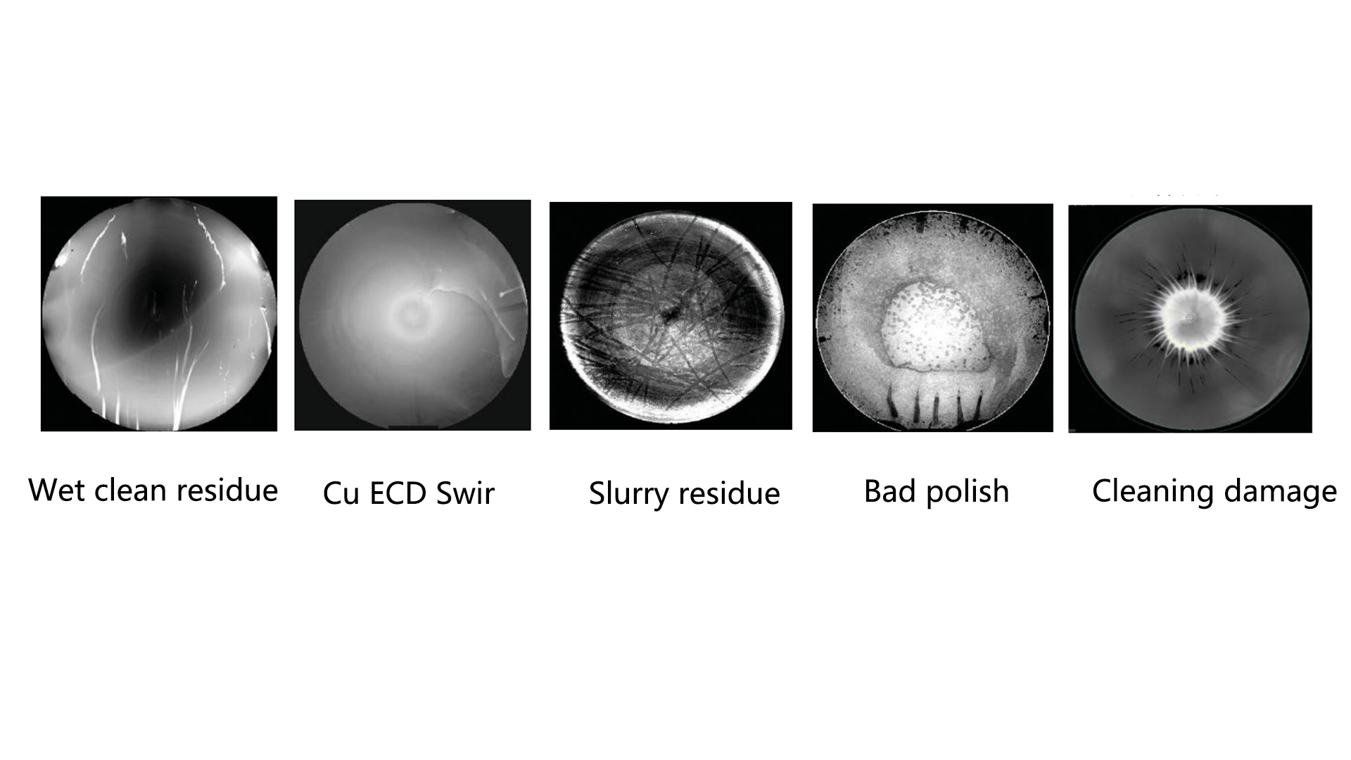
3、 SURFimage™ data channel enables identification of spatially extended surface anomalies, such as local variations in surface micro-roughness, in a full wafer map image. Product manufacturing restarted for increased serviceability and predictability of supply Standardized handler for flexible configurations.
SURFimage Application Examples

Defect Sensitivity
1、Dual Scan is a single recipe option to inspect wafers using both Oblique Illumination for particle detection and Normal Illumination for mechanical scratch and slip detection and automatically combine all results in a single wafer map/results file (SP2XP only).
2、Brightfield Differential Interference Contrast (BF-DIC) improves capture of defects with surface height changes (SP2XP only).
3、Defect & SURFimage results can be combined into a single map output.
4、eXtended Film Sensitivity (XFS) masks helps maximize defect detection on polysilicon, tungsten,and copper (upgrade option).
